
Perovskite-inspired materials
Historically, high-performance semiconductors have been achieved using high-temperature, expensive processing methods to minimise defect densities. Over the past decade, we have witnessed the astonishing rise in performance of lead-halide perovskites in photovoltaics, as well as many other optoelectronic applications, such as light-emitting diodes and X-ray detectors. Surprisingly, these lead-halide perovskites are synthesised via low-temperature methods, which are predicted to significantly more cost-effective than traditional growth techniques. This has prompted the important question of whether the exceptional optoelectronic properties found in lead-halide perovskites can be replicated across other materials systems (i.e., 'perovskite-inspired' materials) , and how such materials could be systematically found.
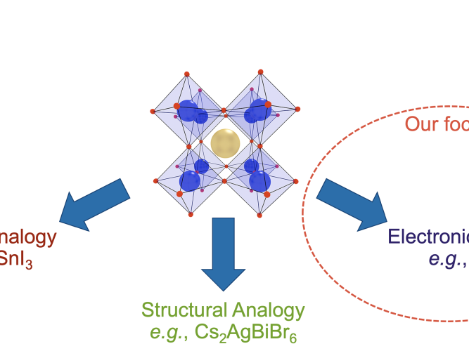
Broadly, there have been three approaches to finding perovskite-inspired materials: 1) chemical analogy (substituting out Pb2+ for alternative divalent cations), 2) structural analogy (finding classes of materials with the perovskite crystal structure), and 3) electronic analogy (which have similar electronic features at the band extrema as lead-halide perovskites), as illustrated in Figure 1. Most groups have focussed on the first and second approaches, whereas we have focussed on the third approach. This has led to us identifying unusual materials that do not necessarily have the perovskite crystal structure.
Defect tolerance
One of the key enabling features of the lead-halide perovskites is their ability to have low rates of non-radiative recombination (i.e., long charge-carrier lifetimes >100 ns) despite having defect densities millions of times higher than silicon, or other traditional semiconductors. This is critical for achieving high efficiencies in devices. For example, in photovoltaics (PVs), light is absorbed to generate electron-hole pairs, which then need to be separated and transported to opposite charge extraction layers. The longer the charge-carrier lifetime, the higher the diffusion (or drift) length, and therefore the higher the fraction of photo-generated charge-carriers that are extracted.
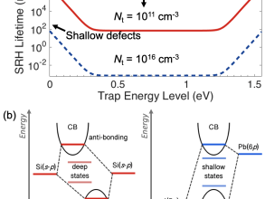
When a defect is present, it can act as a site where electrons and holes are captured and annihilated leading to decreases in PV efficiency. The rate of non-radiative recombination for one defect in a semiconductor can be predicted using the Shockley-Read-Hall (SRH) model. One way of minimising the SRH rate is to minimise defect densities, and this has been the historic approach (i.e., making materials defect-free). With lead-halide perovskites, many computational studies have shown that the main defects form trap levels that are 'shallow', i.e., close to one band-edge. This means that the defect state can easily capture one charge-carrier, but not the other, thus leading to a low SRH rate despite high defect densities being present (Figure 2a). Figure 2b shows a simplified molecular orbital diagram comparing a defect sensitive material (forming deep traps) vs. lead-halide perovskites (forming shallow traps). The electronic structure of lead-halide perovskites was suggested to favour shallow trap formation, and an important reason why this particular electronic structure arises is because of the significant contribution from the valence s electrons from the Pb2+ cation. This led to the hypothesis that key features of the lead-halide perovskite electronic structure may be replicated in compounds based on heavy cations with stable valence s electrons, namely Bi3+, Sb3+, Sn2+ or In+. These materials, termed ns2 compounds, therefore do necessarily have a perovskite crystal structure, but are electronically analogous, and are being explored for whether they can replicate the defect-tolerance found in lead-halide perovskites. It should be noted that these elements have substantially lower toxicity than Pb, especially Bi, which is found in many compounds used in cosmetics or medicines.
We finally add that the electronic structure model for defect tolerance described above was an important starting point, but is an incomplete model for defect tolerance. Developing more in-depth insights into how defect tolerance arises and design rules for identifying materials that could exhibit defect tolerance is a grand challenge for the whole community, and one in which we hope to contribute to addressing.
Electron-phonon coupling
Another important reason behind the exceptional performance of lead-halide perovskites is their decent mobility, which contributes to long diffusion and drift lengths. Whilst the mobility depends on band dispersion, it also depends on how the charge-carriers interact with the lattice. At temperatures above absolute zero, atoms are oscillating from their equilibrium positions, and the quanta for these oscillations are phonons. In a polar semiconductor, charge-carriers can interact with optical phonons (out-of-phase vibrations) to form large polarons. These are called Fröhlich interactions, and result in a reduction in mobility.
There are also acoustic phonons (in-phase vibrations), and charge-carriers coupling to acoustic phonons can be localised to one or a few unit cells, and therefore have substantially lower mobility than expected based on the effective mass. These are called small polarons. Excitons can also undergo a similar process to form self-trapped excitons.
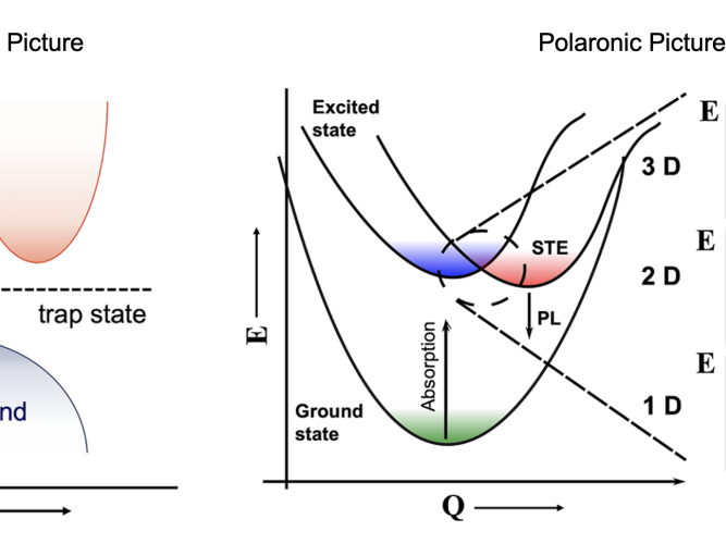
It has been found that 3D lead-halide perovskites form large polarons and do not undergo self-trapping. However, recent work on bismuth-halide semiconductors have found that they almost all undergo carrier localisation. When there is strong coupling between charge-carriers and acoustic phonons, the optoelectronic behaviour can be drastically altered, such that it can no longer be described based on the 'electronic picture', but rather by the 'polaronic picture', i.e., with a configuration coordinate diagram (Figure 3). A configuration coordinate diagram plots the energy of the ground state (dark) and excited state (under illumination) against the average displacement of the atoms from equilibrium (Q). As illustrated in Figure 3, following distortion, there could be a lower energy state that individual charge-carriers or excitons can relax into, in which they are then localised owing to a large energy barrier to the delocalised state. This can lead to a substantial increase in charge-carrier lifetime (from nanoseconds to microseconds) because the charge-carriers remain in this state for a long time and do not annihilate via defect states. Conversely, strong electron-phonon coupling can lead to the introduction of new irreversible loss channels that will still be present even if the material is defect-free.
Strong carrier-phonon coupling therefore limits the performance of photon-harvesting devices. On the other hand, the extra recombination channels introduced through strong carrier-phonon coupling could give rise to luminescence in otherwise non-luminescent materials, and this is beneficial for stable inorganic phosphors. Thus, a critical research effort that has emerged in our group is to understand and control carrier-phonon interactions in perovskite-inspired materials.
New materials
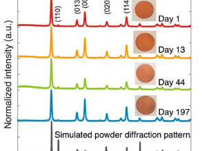
Hundreds of ns2 compounds have been proposed as defect-tolerant, including bismuth oxyiodide (see Chem. Mater., 2017, 29, 4667 for others). Bismuth-based compounds have demonstrated very little evidence of toxicity, bismuth is sufficiently abundant for commercialisation in solar cells, and we recently showed bismuth oxyiodide (BiOI) to be air-stable (Figure 4). We developed an all-inorganic device structure, from which we achieved high external quantum efficiencies that reached up to 80% at 450 nm wavelength, exceeding previous reports of bismuth-based absorbers at the time of publication in 2017 (Adv. Mater., 2017, 29, 1702176). Through computations of the defect diagrams, we found that the dominant point defects in BiOI have shallow transition levels and the material itself to have a high dielectric constant of 45. We followed this up with systematic measurements that showed the electronic structure and optoelectronic properties of BiOI to tolerate percent-level surface defects (Adv. Funct. Mater., 2020, 30(13), 1909983). This experimental evidence is consistent with defect tolerance and is in strong contrast to traditional covalent semiconductors. We also have recent results from spectroscopy and computations suggesting that BiOI may avoid carrier localisation, and indeed we have measured charge-carrier mobilities >80 cm2 V-1 s-1.
Key literature
Review papers
A. M. Ganose, D. O. Scanlon, A. Walsh, R. L. Z. Hoye,* The Defect Challenge of Width-Bandgap Semiconductors for Photovoltaics and Beyond, Nature Communications, Just Accepted
R. L. Z. Hoye,* et al., The Role of Dimensionality on the Optoelectronic Properties of Oxide and Halide Perovskites, and their Halide Derivatives, Advanced Energy Materials, 2021, 12(4), 2100499.
Research papers
R. L. Z. Hoye,* et al., Strongly Enhanced Photovoltaic Performance and Defect Physics of Bismuth Oxyiodide (BiOI), Advanced Materials, 2017, 29(36), 1702176. Press release
T. N. Huq, et al., Electronic Structure and Optoelectronic Properties of Bismuth Oxyiodide Robust against Percent-Level Iodine-, Oxygen-, and Bismuth-Related Surface Defects, Advanced Functional Materials, 2020, 30(13), 1909983.